Micro-Controller - 80C196 In 30 Minutes
Block Diagram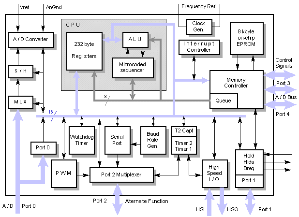
Features
- 16 bit CPU
- 230 bytes of on chip RAM
- 25 Special Function Registers
- Multiple Register Windows
- No accumulator, all register files will act as accumulator
- Built in watchdog timer
- Built in Interrupt controller & Memory controller
- Built in Eight channel ADC
- Built in High Speed Inputs & Outputs
- Built in Pulse width Modulator
- Built in Serial Communication port – UART
- Built in two 16 bit Timers
Addressing Modes
There are 6 addressing modes in 80C196
- Register Direct Addressing Mode
- ADD AX,BX,CX: Add the contents of BX and CX and store
it in AX - ADD AX,BX : Add the contents of AX and AX and store it
in AX - Immediate addressing Mode
- ADD AX,#500h : Add the contents of AX with 500h and store it in AX
- Indirect Addressing Mode
- ADD AX,[BX] : Add the contents of AX with the content of the location indicated by BX, i.e MEM_WORD[BX] and store the result in AX.
- Indirect with Auto Increment Addressing Mode
- ADD AX,[BX]+ : Add the contents of AX with the content of the location indicated by BX, i.e MEM_WORD[BX] and store the result in AX. After that BX register is incremented. For 16bit register the increment will be +2 and for 8 bit register it is +1
- Long Indexed Addressing Mode
- ADD AX,[TBL]BX : Add the contents of AX with the content of the memory location indicated by sum of BX & TBL, i.e MEM_WORD[BX + DIST] and store it in AX. The TBL should be a 16 bit number
- MUL AX,[241]BX : AX ? AX + MEM_WORD[BX + 241]
Watchdog Timer
The watchdog timer is a 16 bit counter that resets the processor when it rolls over to zero. The processor can reset the counter or turn it off, but, correctly used, it will reset the processor in case of a code crash. To avoid getting reset, the program must reset the timer every so often. A program which has crashed will not do so, and the system will reset.
Timers
Two 16 bit timers – Timer0 and Timer1- Which is used to generate pulses, clock signals, to drive high speed output unit (HSO), to identify the high speed input (HSI) event time etc. The timer block diagram is given below

High Speed Input - HSI
The block diagram of HIS is as shown below
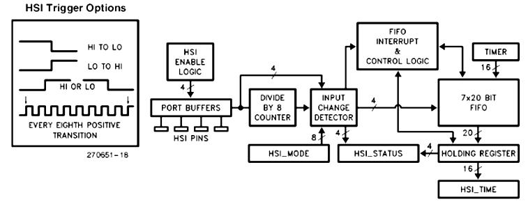
The High Speed Input (HSI) unit can capture the value of Timer1 when an event takes place on one of four input pins (HSI.0-HSI.3). Four types of events can trigger a capture: rising edges only, falling edges only, rising or falling edges, or every eighth rising edge. When events occur, the Timer1 value gets stored in the FIFO along with 4 status bits which indicate the input line(s) that caused the event. The next event ready to be unloaded from the FIFO is placed in the HSI Holding Register, so a total of 8 pieces of data can be stored in the FIFO. Data is taken off the FIFO by reading the HSIÐSTATUS register, followed by reading the HSIÐTIME register. When the time register is read the next FIFO location is loaded into the holding register.
High Speed Output – HSO
The block diagram of HIS is as shown below
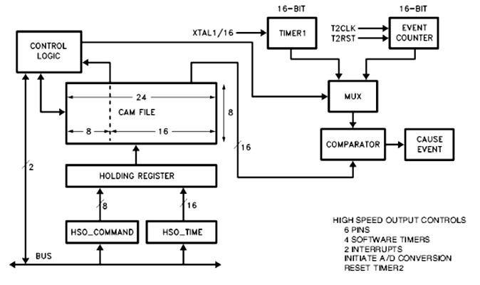
The High Speed Output unit (HSO) trigger events at specific times with minimal CPU overhead. Events are generated by writing commands to the HSOÐCOMMAND register and the relative time at which the events are to occur into the HSOÐTIME register. If it is not locked, when ever the event is occurred that entry will be erased from CAM.
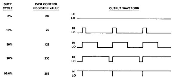
Pulse Width Modulator
The block diagram of HIS is as shown below
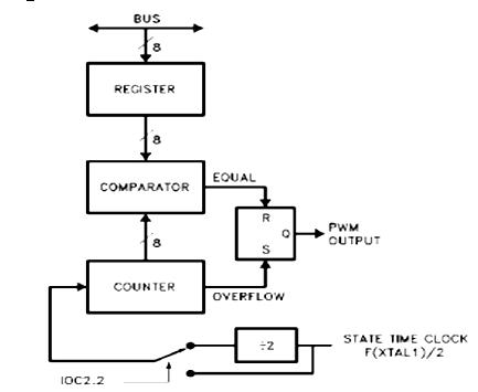
The 8-bit counter is incremented every state time. When it equals 0, the PWM output is set to a one. When the counter matches the value in the PWM register, the output is switched low. When the counter overflows, the output is once again switched high. The pulse width can be controlled by the data which is entering to the PWM register. Typical PWM waves are shown below,
Analog to Digital Converter
The block diagram of HIS is as shown below

Analog Inputs to the 80C196KB System are handled by the A/D converter System. The converter system has an 8 channel multiplexer, a sample-and-hold, and a 10 bit successive approximation A/D converter. Conversions can be performed on one of eight channels, the inputs of which share pins with port 0. A conversion can be done in as little as 91 state times.
Conversions are started by loading the ADÐCOMMAND register at location 02H with the channel number. The conversion can be started immediately by setting the GO bit to a one. If it is cleared the conversion will start when the HSO unit triggers it. The A/D command register must be written to for each conversion, even if the HSO is used as the trigger. The result of the conversion is read in the ADÐRESULT(High) and ADÐRESULT(Low) registers. The ADÐRESULT( High) contains the most significant eight bits of the conversion. The ADÐRESULT(Low) register contains the remaining two bits and the A/D channel number and A/D status.
Serial Port
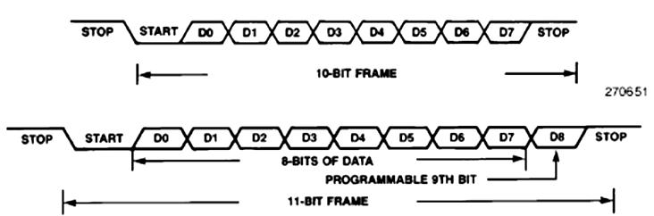
80C196 has one synchronous and 3 asynchronous mode. The asynchronous modes are fully duplex. Mode0 is a synchronous mode which is commonly used for shift register based I/O expansion. In this mode the TXD pin outputs a set of 8 pulses while the RXD pin either transmits or receives data. Data is transferred 8 bits at a time with the LSB first. This is the only mode which uses RXD as an output. Mode1 is the standard asynchronous communications mode. It consists of 10 bits; a start bit (0), 8 data bits (LSB first), and a stop bit (1). Mode2 is the asynchronous 9th bit recognition mode. This mode is commonly used with Mode 3 for multiprocessor communications. It consists of a start bit (0), 9 data bits (LSB first), and a stop bit (1). Parity cannot be enabled in this mode. Mode3 is the asynchronous 9th bit mode. The data frame for this mode is identical to that of Mode2. The transmission differences between Mode3 and Mode2 are that parity can be enabled (PENe1) and cause the 9th data bit to take the even parity value. The TB8 bit can still be used if parity is not enabled (PENe0). When in Mode 3, a reception always causes an interrupt, regardless of the state of the 9th bit. The 9th bit is stored if PENe0 and can be read in bit RB8. If PENe1 then RB8 becomes the Receive Parity Error (RPE) flag.
Interrupts
Twenty-eight (28) sources of interrupts are available on the 80C196KB. These sources are gathered into 15 vectors plus special vectors for NMI, the TRAP instruction, and Unimplemented Opcodes. Three special interrupts are available on the 80C196KB: NMI, TRAP and Unimplemented opcode. The external NMI pin generates an non-maskable interrupt for implementation of critical interrupt routines. The TRAP instruction is useful in the development of custom software debuggers or generation of software interrupts. Five registers control the operation of the interrupt system: INTÐPEND, INTÐPEND1, INTÐMASK and INTÐMASK1 and the PSW which contains a global disable bit.
By SKB


7 Comments (Post a Comment)